Purpose
The RT5759 is a high efficiency synchronous step-down DC-DC converter. Its input voltage range is from 3V to 6V and provides an VID Control regulated output voltage from 0.6V to 1.5V step 10mV while delivering up to 9A of output current. This document explains the function and use of the RT5759 evaluation board (EVB), and provides information to enable operation, modification of the evaluation board and circuit to meet individual requirements.
Introduction
General Product Information
The RT5759 is a high-performance, synchronous stepdown DC-DC converter that can deliver up to 9A output current from a 3V to 6.5V input supply. The output voltage can be programmable from 0.6V to 1.5V with I2C controlled 7-Bits VID. The device integrates low RDS(ON) power MOSFETs and an integrated diode of bootstrap circuit to offer a very compact solution.
The RT5759 adopts Advanced Constant On-Time (ACOT®) control architecture that provides ultrafast transient response and further reduce the external-component count. In steady states, the ACOT® operates in nearly constant switching frequency over line, load and output voltage ranges and makes the EMI filter design easier. The RT5759 offers automatic PSM that maintains high efficiency during light load operation. The RT5759 can also operate in Forced-CCM through I2C setting that helps meet tight voltage regulation accuracy requirements.
The device offers a variety of functions for more design flexibility. The switching frequency, current limit level and over temperature threshold are selectable via I2C. Independent enable control input pin and power good indicator are also provided for easy sequence control. Besides, the designers can also command the device to be enabled or shutdown via the I2C interface.
The device offers Independent enable control input pin and power good indicator for easily sequence control. To control the inrush current during the startup, the device provides a programmable soft-start up by an external capacitor connected to the SS pin. Fully protection features are also integrated in the device including the cycle-by-cycle current limit control, UVP, input UVLO and OTP.
The RT5759 is available in a thermally enhanced UQFN-13L 3x3 (FC) package.
Product Feature
- Dramatically Fast Transient Response
- Steady 1MHz ±20% Switching Frequency
- Advanced COT Control Loop
- Optimized for Ceramic Output Capacitors
- 3V to 6.5V Input Voltage Range
- Integrated 12mΩ/8mΩ MOSFETs
- Internal Start-Up into Pre-Biased Outputs
- Power Good Indicator
- Enable Control
- Over-Current and Over-Temperature Protections
- Under-Voltage Protection with Hiccup Mode
- VID Control Range Via I2C Compatible Interface : 0.6V to 1.5V step = 10mV
Key Performance Summary Table
|
Key Features
|
Evaluation Board Number : PCB105_V1
|
|
Default Input Voltage
|
3.3V
|
|
Maximum Output Current
|
9A
|
|
Default Output Voltage
|
1.0V
|
|
Default Marking & Package Type
|
RT5759GQUF, UQFN-13L 3x3 (FC)
|
|
Operation Frequency
|
Steady 1MHz in CCM Mode
|
Bench Test Setup Conditions
Headers Description and Placement
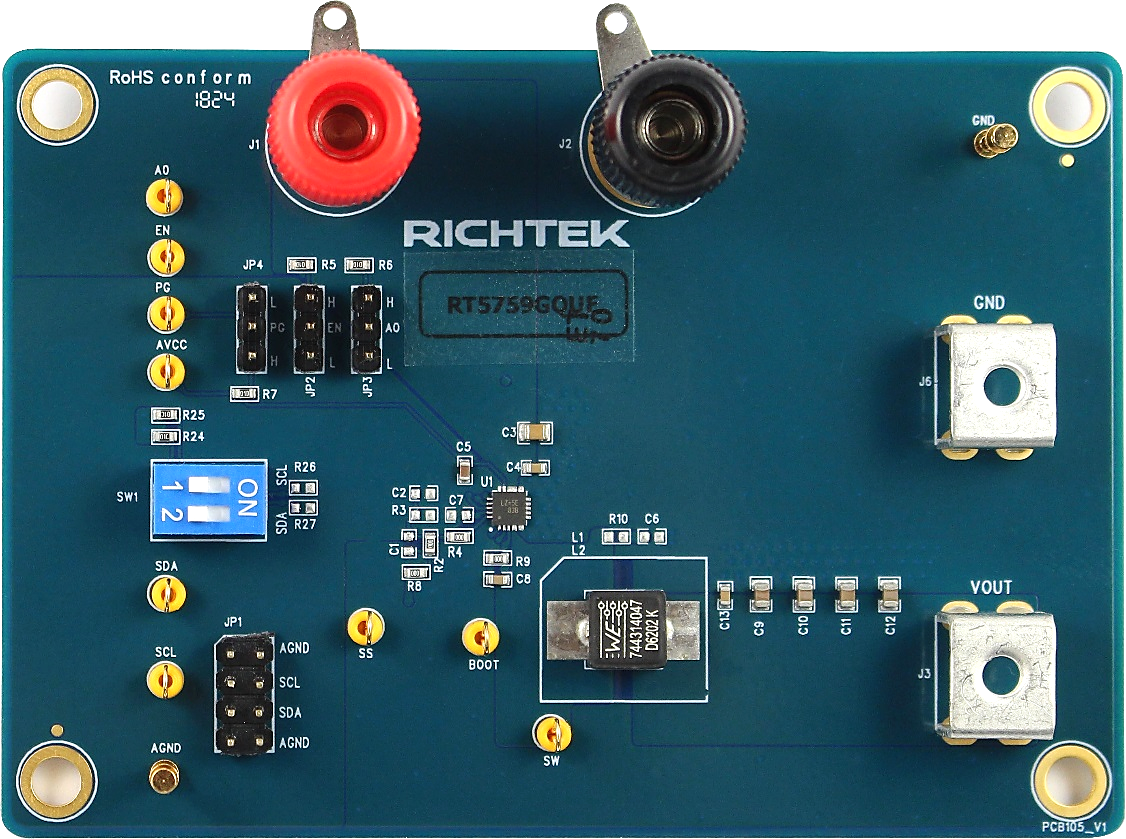
Carefully inspect all the components used in the EVB according to the following Bill of Materials table, and then make sure all the components are undamaged and correctly installed. If there is any missing or damaged component, which may occur during transportation, please contact our distributors or e-mail us at evb_service@richtek.com.
Test Points
The EVB is provided with the test points and pin names listed in the table below.
|
Test point/
Pin Name
|
Signal
|
Comment (expected waveforms or voltage levels on test points)
|
|
EN
|
Enable Control Input
|
Enable control input. A logic-high enables the converter; a logic-low forces the device into shutdown mode. EN can be connected to VIN for automatic start-up.
|
|
A0
|
I2C Setting
Device address select pin.
|
High : 0x60, Low : 0x63, Floating : 0x62.
|
|
BOOT
|
Bootstrap
|
Supply for high-side gate driver. Connect a 0.1µF ceramic capacitor between BOOT and SW pins.
|
|
SW
|
Switch Node
|
Switch node. Connect this pin to an external L-C filter.
|
|
PGND
|
Power Ground
|
Used for all large signal grounds.The exposed pad must be soldered to a large PCB copper area for maximum power dissipation.
|
|
VIN
|
Input Voltage
|
Support 3V to 6.5V input voltage. Connect this pin with a suitable
capacitance for noise decoupling. The bypass capacitor should be placed as close to VIN pin as possible.
|
|
AVCC
|
Output for Internal Analog Power
|
Connect a 4.7µF capacitor as close to the VCC pin as possible.
|
|
AGND
|
Analog GND
|
Signal ground of the FB network. AGND and PGND are connected with a short trace and at only one point to reduce circulating currents.
|
|
PGOOD
|
Power Good Indicator Output
|
This pin has an open drain structure. Pull this pin high to a voltage source with a 100kΩ resistor.
|
|
SDA
|
I2C interface
|
DATA.
|
|
SCL
|
I2C interface
|
CLK.
|
|
SS
|
Soft-Start Time Control Pin
|
Connect a capacitor between the SS pin and AGND to set the soft-start time. The default internal start-up time is 1.6ms without external capacitor.
|
|
FB
|
Feedback Input
|
The pin is used to set the output voltage of the converter via a resistor divider. Suggest placing the FB resistor divider as close to FB pin and AGND as possible. Keep away from high current loops and swithing voltages.
|
Power-up & Measurement Procedure
1. Apply a 3.3V/5V nominal input power supply (3V < VIN < 6.5V) to the VIN and GND terminals.
2. Set the jumper at JP2 to connect terminals H and EN, connecting EN to VIN through resistor R5 (100kΩ). The Enable pin can connected to VIN directly as well to enable operation.
3. Set the jumper at JP4 to connect terminals H and PG, Connenting AVCC to H through resistor R7 (100kΩ).
4. Both of the CP2 and CP3 are short.
5. Verify the output voltage (approximately 1V) between VOUT and GND.
6. Connect an external load up to 9A to the VOUT and GND terminals and verify the output voltage and current.
Schematic, Bill of Materials & Board Layout
EVB Schematic Diagram
RT5759HGQW demo board : VIN = 3.3V / 5V, VOUT 1.0V / 9A
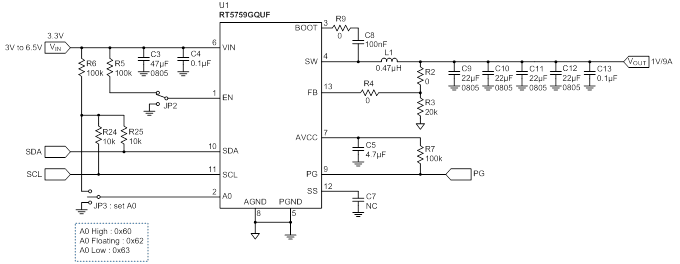
* Note :
1. The capacitance values of the input and output capacitors will influence the input and output voltage ripple.
2. MLCC capacitors have degrading capacitance at DC bias voltage, and especially smaller size MLCC capacitors will have much lower capacitance than specified :
3. MLCC 22µF/6.3V/X5R 0805 size will have ~13.6µF capacitance @ 1V DC bias and AC ripple effect.
4. MLCC 22µF/16V/X5R 0805 size will have ~8.18µF/11.75µF @ 5V/3.3V DC bias and AC ripple effect.
5. MLCC 47µF/10V/X5R 0805 size will have ~12.88µF/19.76µF @ 5V/3.3V DC bias and AC ripple effect.
6. Set default soft start time 1.6ms by C7 NC.
Bill of Materials
|
Reference
|
Qty
|
Part Number
|
Description
|
Package
|
Manufacturer
|
|
U1
|
1
|
RT5759GQUF
|
Step-Down DC-DC Converter
|
UQFN-13L 3x3 (FC)
|
RICHTEK
|
|
C3
|
1
|
GRM21BR61A476ME15L
|
47µF/10V/X5R
|
C-0805
|
MURATA
|
|
C4, C8, C13
|
3
|
C1608X7R1H104K080AA
|
100nF/50V/X7R
|
C-0603
|
TDK
|
|
C5
|
1
|
C1608X5R0J475K080AB
|
4.7µF/6.3V/X5R
|
C-0603
|
TDK
|
|
C9, C10, C11, C12
|
4
|
GRM21BR60J226ME39
|
22µF/6.3V
|
C-0805
|
MURATA
|
|
L1
|
1
|
WURTH 744314047
|
0.47µH
|
6.9x6.9x4.8mm
|
WE
|
|
R2, R4, R9
|
3
|
WR06X000 PTL
|
0
|
R-0603
|
WALSIN
|
|
R3
|
1
|
RTT032002FTP
|
20k
|
R-0603
|
RALEC
|
|
R5, R6, R7
|
3
|
WR06X1003FTL
|
100k
|
R-0603
|
WALSIN
|
|
R24, R25
|
2
|
WR06X1002FTL
|
10k
|
R-0603
|
WALSIN
|
|
|
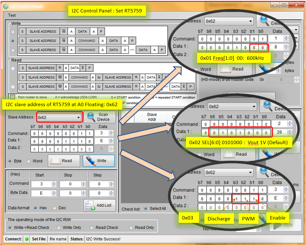
The RT5759 is I2C controlled : The parameters were set via Richtek I2C tool :
fSW = 600kHz
VOUT = 1V
Mode = Forced-PWM
|
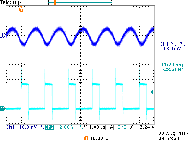
Measurement Results
PWM mode, 600kHz
|
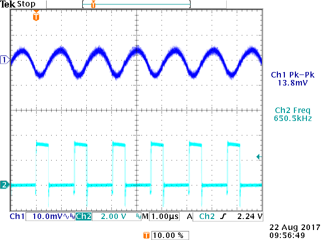
Output ripple measurement at VIN = 3.3V 10mA load
CH1 : VOUT , CH2 : VSW
|
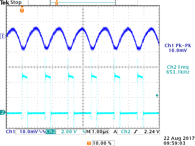
Output ripple measurement at VIN = 3.3V 2A load
CH1 : VOUT , CH2 : VSW
|
|
|
|
|
Output ripple at 10mA load : 13.4mVpp
|
Output ripple at 2A load : 13.8mVpp
|
|
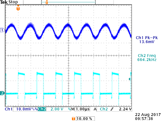
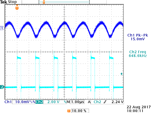
Output ripple measurement at VIN = 3.3V 6A load
CH1 : VOUT , CH2 : VSW
|
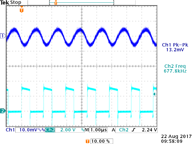
Output ripple measurement at VIN = 3.3V 9A load
CH1 : VOUT , CH2 : VSW
|
|
|
|
|
Output ripple at 6A load : 13.6mVpp
|
Output ripple at 9A load : 13.2mVpp
|
|
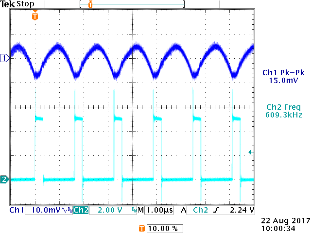
Output ripple measurement at VIN = 5V 10mA load
CH1 : VOUT , CH2 : VSW
|
Output ripple measurement at VIN = 5V 2A load
CH1 : VOUT , CH2 : VSW
|
|
|
|
|
Output ripple at 10mA load : 15mVpp
|
Output ripple at 2A load : 15mVpp
|
|
Output ripple measurement at VIN = 5V 6A load
CH1 : VOUT , CH2 : VSW
|
Output ripple measurement at VIN = 5V 9A load
CH1 : VOUT , CH2 : VSW
|
|

|
|
|
Output ripple at 6A load : 15.4mVpp
|
Output ripple at 9A load : 16mVpp
|
|
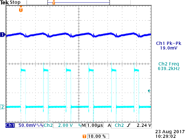
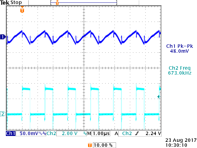
VIN ripple measurement at VIN = 5V 2A load
CH1 : VOUT , CH2 : VSW
|
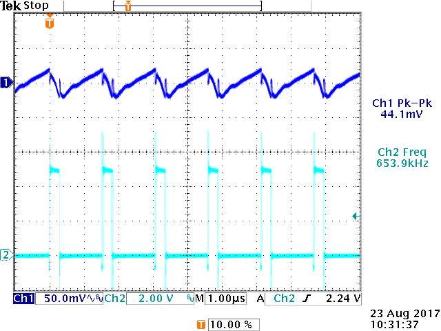
Vin ripple measurement at VIN = 5V 8A load
CH1 : VOUT , CH2 : VSW
|
|
|
|
|
VIN Ripple at 2A load : 19mVpp
|
VIN Ripple at 8A load : 44.1mVpp
|
|
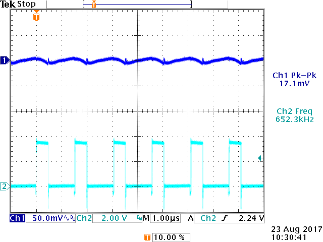
VIN ripple measurement at VIN = 3.3V 2A load
CH1 : VOUT , CH2 : VSW
|
VIN ripple measurement at VIN = 3.3V 8A load
CH1 : VOUT , CH2 : VSW
|
|
|
|
|
VIN Ripple at 2A load : 17.1mVpp
|
VIN Ripple at 8A load : 48mVpp
|
|
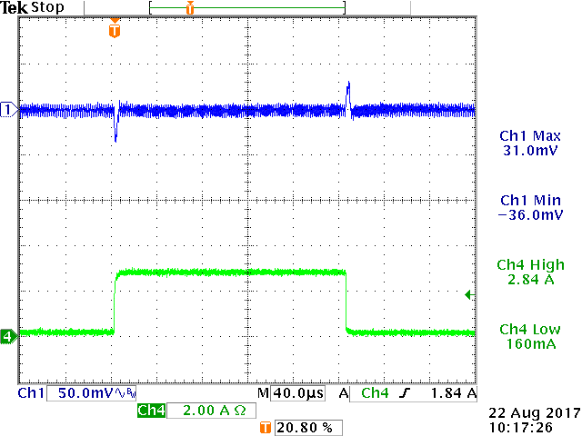
Dynamic load 160mA to 2.84A load step (PWM mode)
CH1 : VOUT, CH4 : IOUT
|
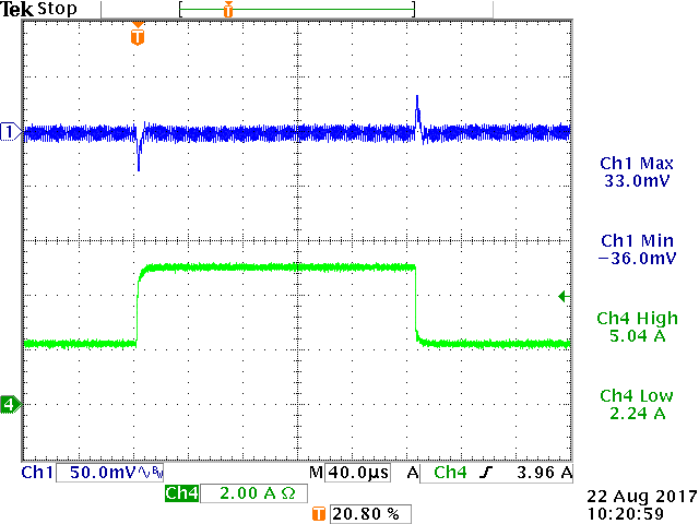
Dynamic load 2.24A to 5A load step (PWM mode)
CH1 : VOUT, CH4 : IOUT
|
|
|
|
|
Overshoot : 31mV, undershoot : 36mV
|
Overshoot : 33mV, undershoot : 36mV
|
|
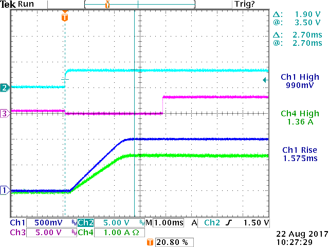
Start-up measurement from Enable : EN pin low to high
CH1 : VOUT, CH2 : VEN, CH3 : VPG, CH4 : IOUT
|
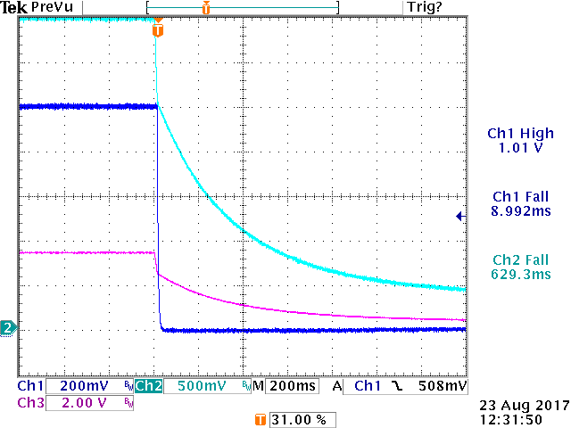
Power off measurement from V-in : VIN from 3.3V to 0V
CH1 : VOUT, CH2 : VIN, CH3 : VPG
|
|
|
|
|
Start-up time 2.7msec. Soft-start 1.575msec
|
VOUT discharge during power off
|
|
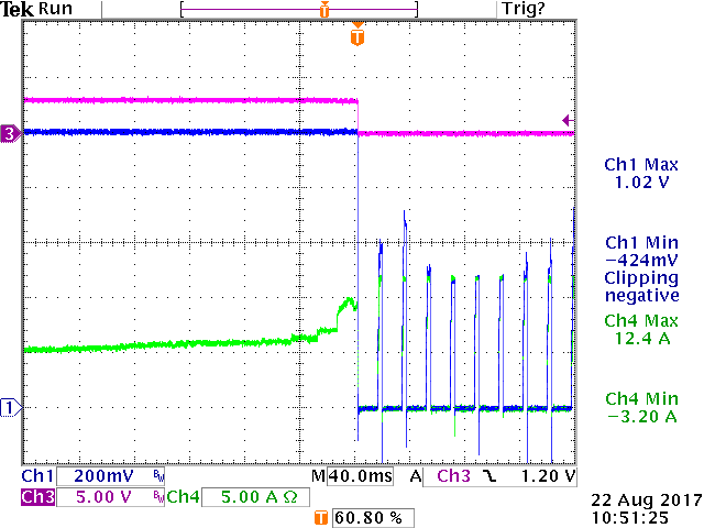
OCP measurement : Gradually increase load
CH1 : VOUT, CH3 : VPG, CH4 : IOUT
|
|
|
|
Auto-recovery hiccup mode when OC limit is exceeded.
|
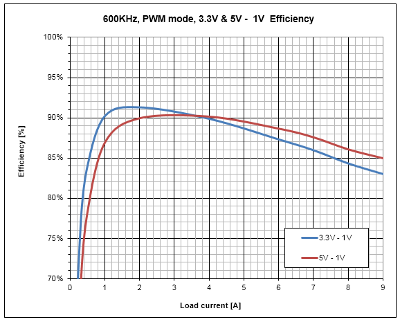
Efficiency : 600kHz, PWM mode
|
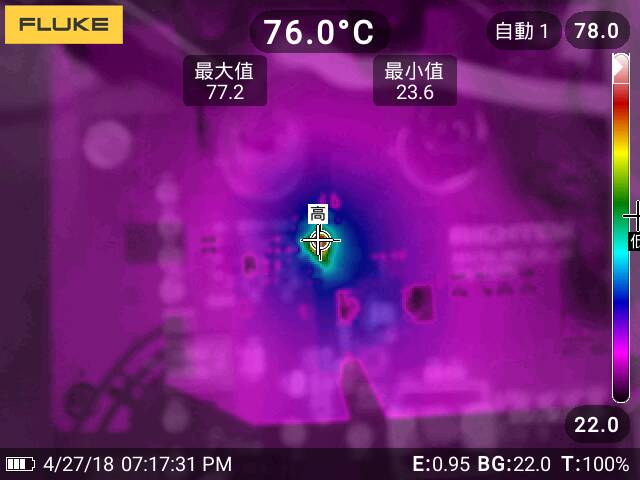
IC top temperature = 76°C on VIN = 3.3V, VOUT = 1V, IOUT = 9A
|
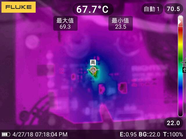
IC top temperature = 67.7°C on VIN = 5V, VOUT = 1V, IOUT = 9A
|
|
|
|
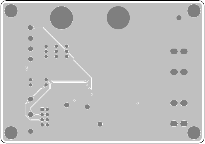
PCB Layout
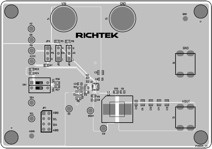
Top View (1st layer)
PCB Layout—Inner Side (2nd Layer)
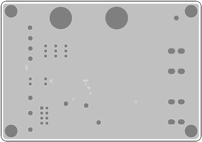
PCB Layout—Inner Side (3rd Layer)
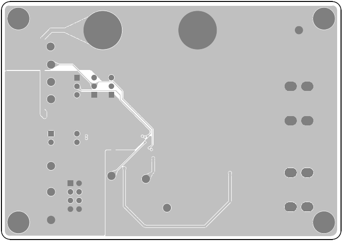
Bottom View (4th Layer)